| By Haiqi Li |
Semiconductors play a critical role in powering a wide range of cutting-edge digital devices and are essential technology enablers. The global semiconductor industry is poised to continue its strong growth trajectory over the next decade, fueled by advances in emerging technologies such as autonomous driving, artificial intelligence (AI), 5G, and the Internet of Things (IoT), as well as sustained investment in research and development and intensified competition among leading industry players. The two main types of semiconductor products are Integrated Circuit and Discrete semiconductors. In 2022, the Discrete semiconductors market is expected to reach $34 billion, representing 4.6% of the entire semiconductor market.[1]
Discrete power devices are a crucial component in enabling the development of power converters and systems. They play a key role in precisely managing electrical energy from the source to the load, while ensuring high efficiency and exceptional reliability based on the load demand. These devices are vital for extending the battery life of portable electronics. Emerging wide-bandgap power devices offer low- and high-power applications at higher frequencies, catering to consumer electronics and higher-power applications in the energy, transportation, and automotive sectors. Power diodes, thyristors, power metal-oxide-semiconductor field effect transistors (MOSFETs), and insulated gate bipolar transistors (IGBTs) are some examples of important power devices.[2] To manufacture these specialty devices at a low cost, reliable and cost-effective material is required.
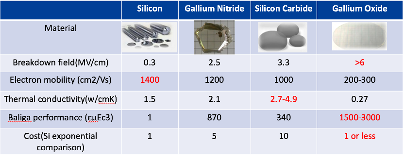
Power devices are composed of different materials such as silicon, Gallium Nitride, Silicon Carbide, and Gallium Oxide, each with unique properties. Among these materials, Gallium(III) Oxide is an ultra-wide bandgap semiconductor and inorganic compound with the chemical formula Ga2O3. It is currently being actively researched for use in power electronics, gas sensing, and phosphors. [3]The compound exists in several polymorphs, with the monoclinic β-phase being the most stable. Gallium(III) Oxide stands out for its very high breakdown electric field, which refers to the critical electric field strength at which a semiconductor material experiences breakdown and a rapid increase in current occurs (E > 6 MV cm−1). This is significantly higher compared to the traditional Si (0.3 MV cm−1) and later developed SiC (3.3 MV cm−1) materials.
Silicon with the highest electron mobility can provide the highest conductivity and perform better in high-frequency applications. Moreover, electron mobility is closely linked to device characteristics, including response time and power consumption, and higher electron mobility materials typically exhibit faster response times and lower power consumption. Consequently, Gallium Oxide displays a significantly larger Baliga’s figure of merit (BFOM). BFOM = εμE3b; where ε represents the relative dielectric constant, and μ denotes the electron mobility[4]. BFOM is a crucial criterion used to evaluate a material’s suitability for use in power devices. Higher BFOM values indicate better performance of power semiconductor devices.
During operation, semiconductor devices produce heat, and materials with high thermal conductivity can efficiently transfer heat, leading to lower operating temperatures of the device. This not only enhances the device’s performance but also increases its reliability. Despite having the lowest thermal conductivity among the four materials, Gallium(III) Oxide is still suitable for use in most applications since most semiconductor devices operate below 250℃. At this temperature range, the performance of Gallium(III) Oxide is unlikely to exhibit significant degradation.
Gallium(III) Oxide can be easily grown using low-cost, atmospheric pressure melt-growth methods that are suitable for mass production. The cost of these methods is only one-fifth that of GaN and comparable to that of Silicon. This makes Gallium(III) Oxide superior in terms of high-quality single-crystal growth. As a result, Gallium(III) Oxide is a highly promising material for the development of next-generation high-power semiconductor devices.

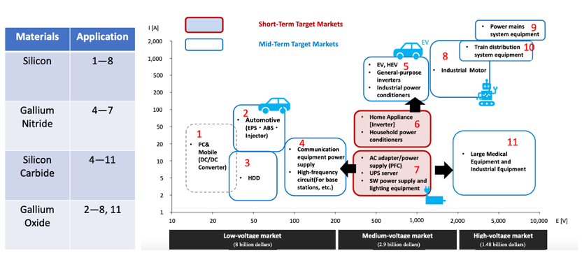
According to its characteristics, Gallium Oxide may initially be applied in home appliances before moving into the automotive industry. Currently, the Gallium Oxide market mainly focuses on the medium-voltage market, which is valued at 2.9 billion dollars. [5]However, this technology is not yet fully matured and requires further testing. Furthermore, Gallium Oxide has the potential to create a larger market in the new energy vehicle industry. Despite its potential, it is unlikely that Gallium Oxide will completely replace Silicon due to Silicon’s superior electron mobility, which is crucial for PC and mobile devices. Additionally, Gallium Oxide’s relatively poor thermal conductivity may limit its use in power and train distribution systems.

Gallium(III) Oxide currently has a relatively small market size in the semiconductor industry. However, it is expected to grow significantly to reach a market size of $1542 million by 2030, with a compound annual growth rate (CAGR) of 66.9% during the forecast period from 2021 to 2030. [6]The unique properties of Gallium(III) Oxide, such as high critical electric-field strength and band gap, make it an attractive option for the semiconductor industry. The primary market driver for Gallium(III) Oxide is the rapid expansion of the automobile industry. Additionally, replacing existing materials such as Gallium Nitride and Silicon Carbide would also contribute to market growth. Although Ga2O3-device technology is still in the research stage, it is reaching critical mass, and researchers are exploring potential applications for fast switches, multi-kilovolt power transistors, and RF devices.

Despite the ongoing development of vertical Gallium(III) Oxide devices, there are several challenges at both the device and material level that must be addressed to accelerate their development and establish them as a viable commercial technology. Several areas require research efforts to provide significant breakthroughs in Gallium(III) Oxide, including P-type doping and Gate-Dielectric.[7]
It is hard to use Gallium(III) Oxide to make P-type semiconductors. Without p-type conductivity, it may be challenging to take full advantage of the benefits of Gallium(III) Oxide. P-n junctions serve as the fundamental component of nearly all vertical power devices and function as the voltage-blocking module. Gate-dielectrics are important and sensitive parts of the power MOSFETs. The electric field experienced by the gate-dielectric should not exceed one-third of the total critical electric field capability. However, this can be challenging as high-k and high critical electric field capability are inversely proportional.
Gallium oxide technology has developed rapidly in the past decade. Its excellent performance and low cost would make power semiconductor products more affordable in the future.
[1]“SEMICONDUCTOR INDUSTRY ASSOCIATION FACTBOOK”, Semiconductor Industry Association, https://www.semiconductors.org/resources/factbook/
[2] Discretes & Power Devices Solutions, Lam research, https://www.lamresearch.com/products/our-solutions/discretes-power-devices-solutions/
[3] Gallium(III) oxide, Wikipedia,https://en.wikipedia.org/wiki/Gallium(III)_oxide
[4] W. Li, K. Nomoto, Z. Hu, T. Nakamura, D. Jena, and H. G. Xing, in 2019 IEEE International Electron Devices Meeting (IEDM) (IEEE, 2019), pp. 12.4.1–12.4.4.
[5]Flosfia, https://flosfia.com/struct/wp-content/uploads/Corporate-Profile_English_2021-April_Web-Page2.pdf
[6] Fuji Economy “Current status and future of the market for Next-Generation Power Devices and Power Electronics-Related equipment”, https://flosfia.com/struct/wp-content/uploads/Corporate-Profile_English_2021-April_Web-Page2.pdf
[7] Vertical GaN and Vertical Ga2O3 Power Transistors: Status and Challenges, https://onlinelibrary.wiley.com/doi/full/10.1002/pssa.202100659
 Previous post
Global Warming Exacerbates Africa Drought


